
If you're involved with processors or semiconductor technology, you're probably familiar with TSMC. The world's leading contract chip manufacturer recently unveiled its next development step at its North America Technology Symposium: the 1.4-nanometer process known as A14, which is scheduled to enter mass production in 2028. With this, TSMC is continuing its technological roadmap and is specifically targeting partners like Apple, who regularly rely on the latest manufacturing technologies.
TSMC produces chips for many major tech companies, including Nvidia, AMD, Qualcomm, and, above all, Apple. Apple, in particular, has relied on TSMC's manufacturing expertise for its A and M chips for years. This close partnership makes it very likely that Apple will gain early access to the new 1.4nm process. Apple currently relies on chips with a 3nm structure width, but the switch to 2nm is planned for 2026. The A14 process will then mark the next step two years later.
What the A14 process can do
TSMC's new A14 process is based on a 1.4-nanometer structure width. Compared to the upcoming 2nm (N2) technology, TSMC says it offers three key advantages:
- Up to 15 percent higher performance with the same energy consumption
- Or up to 30 percent less power consumption with the same performance
- Additionally, a logic density that is over 20 percent higher
These technological advances mean that chips are becoming smaller, more efficient, and more powerful. This is particularly important for mobile devices such as smartphones, tablets, and laptops, where energy efficiency and space requirements are crucial.
New cell architecture: NanoFlex Pro
As part of the launch, TSMC also announced a further development of its existing standard cell architecture. The new platform is called NanoFlex Pro and is intended to extend the existing NanoFlex architecture. The goal is to enable higher performance, better energy efficiency, and greater design flexibility for customers through this optimization. This architecture will enable developers to design more efficient chips with variable power consumption and complexity, which should support the long-term development of AI applications and high-end SoCs.
Schedule and outlook
The A14 node is scheduled for series production in 2028. It is not yet clear which customers will have access to the new technology first. However, due to the close collaboration between Apple and TSMC, it is conceivable that Apple will be at the forefront once the A14 process is ready for production. Before that, however, TSMC will introduce its 2nm process (N2) to the market. Mass production is scheduled to begin in 2025. Apple plans to launch the first devices with 2nm technology starting in 2026. The iPhone 18 series is expected to be the first to use the A20 chip based on this manufacturing process. Until then, Apple will continue to use the 3nm node (N3P) for iPhones and Macs, primarily due to the currently limited production capacities and the high costs of 2nm chips (via businesswire).
TSMC sets new standards for Apple and Co.
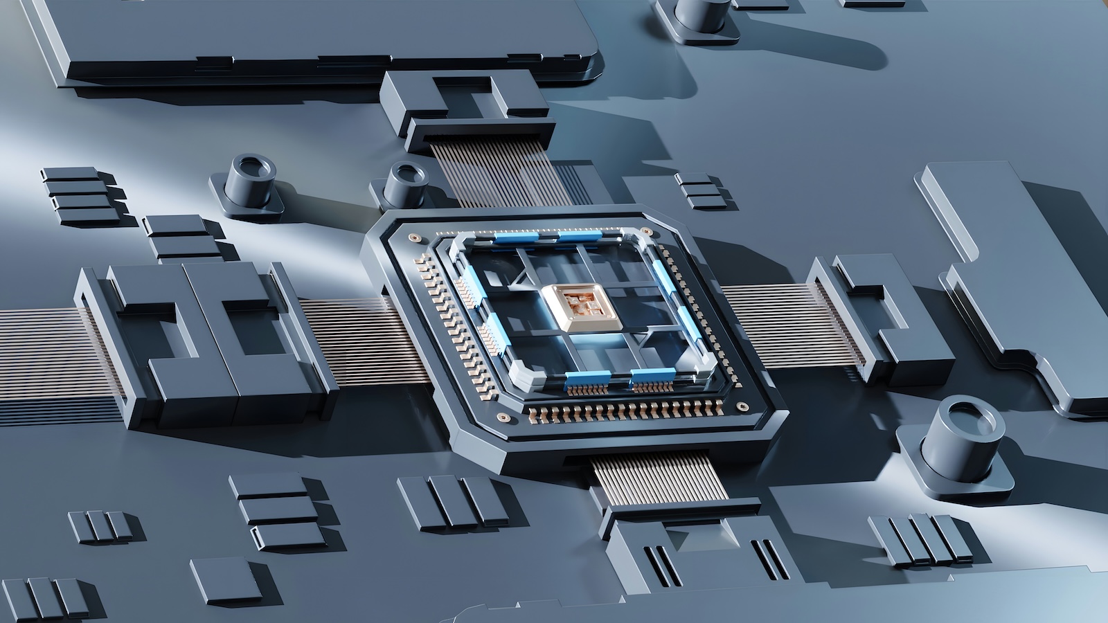
With the 1.4nm A14 process, TSMC demonstrates that technological progress in semiconductors doesn't stop even after 2nm. The new node promises more performance, higher efficiency, and more compact designs. This is likely to be an important step for Apple and other innovation leaders in bringing powerful and energy-efficient devices to market in the future. Anyone interested in the future of the semiconductor industry should therefore continue to keep a close eye on TSMC. (Photo by Unsplash+ / Osarugue Igbinoba)
- EU attacks Apple: US speaks of targeted discrimination
- Apple and Trump contacts: Senator calls for transparency
- Apple under pressure: EU imposes €500 million fine